How to Address Impedance Control in HDI PCBs
Impedance Control in HDI PCBs
High-Density Interconnection printed circuit boards, or HDI PCBs, are becoming increasingly popular as manufacturers strive to improve the quality of their products and keep them smaller and lighter. This technology allows for increased components and more advanced features in a much smaller space.
hdi circuit board utilize microvias, thinner traces and other design techniques to achieve higher signal levels with lower power consumption. They can also reduce the number of layers required, which cuts down on manufacturing costs and assembly time. These advantages, along with the fact that they deliver superior reliability and performance, make them an ideal choice for high-end gadgets and consumer electronics.
As the demand for more powerful devices continues to grow, it has become necessary to develop new technologies that will allow us to pack more into a smaller space. The HDI circuit board is one of the latest and most advanced. It is designed to meet the growing demands for compact electronic devices that are faster, more reliable and have improved signal integrity. It does this by reducing the amount of wiring required to connect components and shortening the distance between signals.
How to Address Impedance Control in HDI PCBs
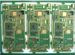
A HDI circuit board consists of several layers that are sandwiched together and connected with copper-etching technology that is continually refined for precision. The most common material used is FR4, but there are other options depending on the application. Surface finishes include ENIG, HASL, immersion tin and gold. The number of sequential laminations and the type of via structure are other important considerations when designing an HDI circuit board.
The first step in implementing an HDI design is to select the components that will be used. Then, a layout is created that utilizes the available space. This layout will need to include the number of components and the size of their pins, as well as the amount of space needed for signal routing. It will also need to be able to incorporate the appropriate layer stack-ups and the number of vias and through-holes needed.
Getting the most out of your HDI design requires careful planning. This is especially true when it comes to routing impedance controlled traces. You need to use your routing tools to create an impedance profile and keep your manufacturer’s DFM rules in mind as you route the traces. You can also take advantage of the online DRC engine in your routing software to help ensure that you are meeting your fabrication process’s requirements for impedance control.
A HDI circuit board can be used in a wide range of devices. It is a great option for advanced technology systems like smartphones and games consoles, as well as medical equipment such as miniature-sized cameras that can be used for patient diagnosis. They are also widely used in communications devices like routers, switches and semiconductor modules. In fact, it’s nearly impossible to find a modern gadget that doesn’t contain an HDI circuit board! If you’re looking to bring your own product to life, ABL Circuits can help you with the design and manufacture of your HDI circuit board.